- 您现在的位置:买卖IC网 > Sheet目录2002 > LTC1096IN8#PBF (Linear Technology)IC A/D CONV 8BIT SRL IN/OUT 8DIP
LTC1096/LTC1096L
LTC1098/LTC1098L
17
10968fc
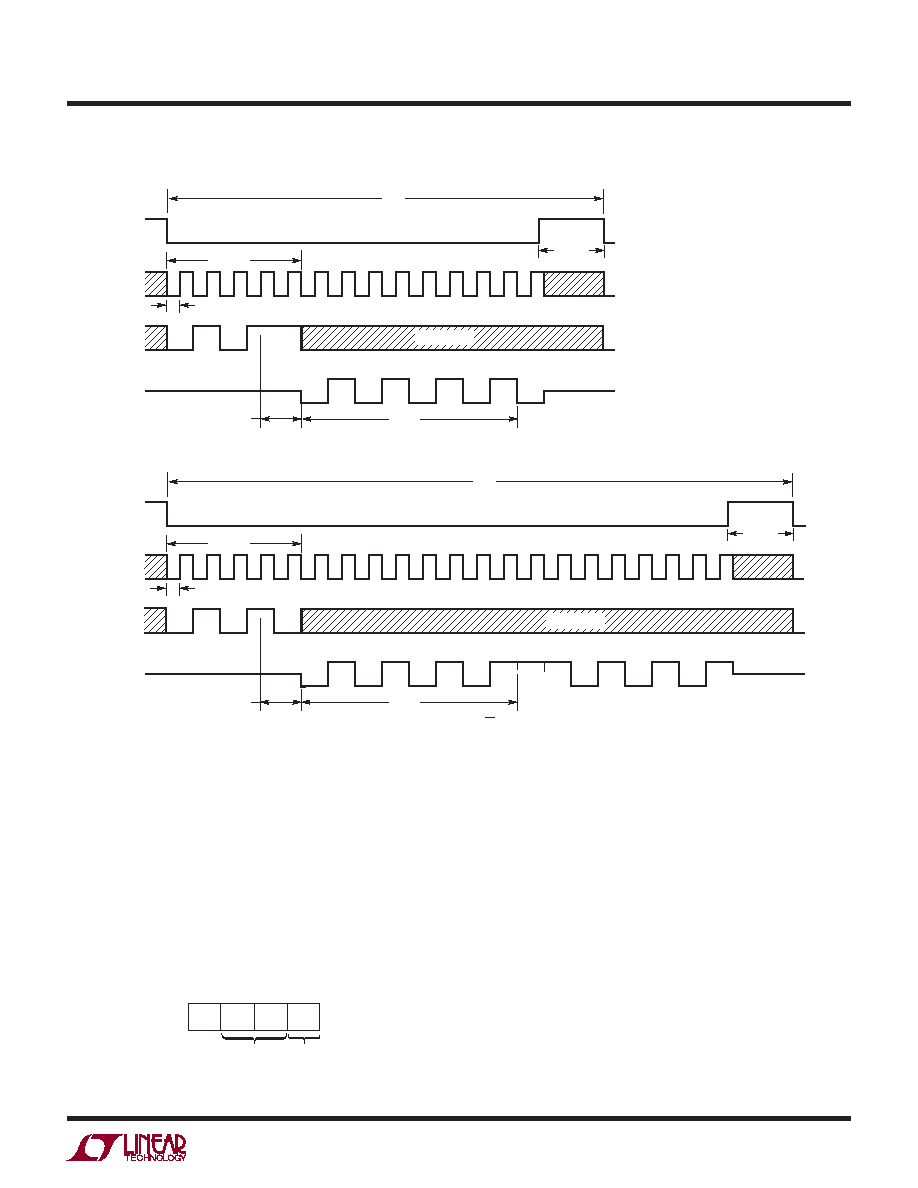
Input Data Word
The LTC1096(L) requires no DIN word. It is permanently
congured to have a single differential input. The conver-
sion result, in which output on the DOUT line is MSB-rst
sequence, followed by LSB sequence providing easy
interface to MSB- or LSB-rst serial ports.
The LTC1098(L) clocks data into the DIN input on the ris-
ing edge of the clock. The input data words are dened
as follows:
Start Bit
The rst “logical one” clocked into the DIN input after CS
goes low is the start bit. The start bit initiates the data
transfer. The LTC1098(L) will ignore all leading zeros which
precede this logical one. After the start bit is received,
the remaining bits of the input word will be clocked in.
Further inputs on the DIN pin are then ignored until the
next CS cycle.
APPLICATIONS INFORMATION
CLK
CS
tCYC
POWER
DOWN
tsuCS
tWAKEUP
DIN
SGL/
DIFF
MSBF
B0*
B1
B2
B3
B4
B5
B6
B7
NULL
BIT
Hi-Z
DOUT
tCONV
tSMPL
HI-Z
START
ODD/
SIGN
DON'T CARE
MSB-FIRST DATA (MSBF = 0)
MSB-FIRST DATA (MSBF = 1)
10968 F02
CLK
CS
tCYC
POWER
DOWN
tsuCS
tWAKEUP
DIN
SGL/
DIFF
MSBF
B0
B1
B2
B3
B4
B5
B6
B7
NULL
BIT
Hi-Z
DOUT
tCONV
tSMPL
HI-Z
START
ODD/
SIGN
DON'T CARE
B7*
B6
B5
B4
B3
B2
B1
*AFTER COMPLETING THE DATA TRANSFER, IF FURTHER CLOCKS ARE APPLIED WITH CS LOW, THE ADC WILL OUTPUT ZEROS INDEFINITELY.
(MSB)
Figure 2. LTC1098(L) Operating Sequence Example: Differential Inputs (CH+, CH–)
SGL/
DIFF
ODD/
SIGN
MSBF
START
MUX
ADDRESS
MSB-FIRST/
LSB-FIRST
10968 AI02
发布紧急采购,3分钟左右您将得到回复。
相关PDF资料
LTC1099ACN#PBF
IC A/D CONV 8BIT HI-SPEED 20-DIP
LTC1197IMS8#PBF
IC ADC 10BIT 500KHZ SHTDWN 8MSOP
LTC1198-1BCS8#PBF
IC ADC 8BIT 750KHZ SAMPL 8-SOIC
LTC1257IS8#TRPBF
IC D/A CONV 12BIT VOLT OUT 8SOIC
LTC1276ACN#PBF
IC A/D CONV 12BIT SAMPLING 24DIP
LTC1278-4IN#PBF
IC A/DCONV SAMPLNG W/SHTDN 24DIP
LTC1279CG#TRPBF
IC A/DCONV SAMPLNG W/SHTDN24SSOP
LTC1282ACN#PBF
IC A/D CONV SAMPLING W/REF 24DIP
相关代理商/技术参数
LTC1096IN8-PBF
制造商:LINER 制造商全称:Linear Technology 功能描述:Micropower Sampling 8-Bit Serial I/O A/D Converters
LTC1096IN8-TR
制造商:LINER 制造商全称:Linear Technology 功能描述:Micropower Sampling 8-Bit Serial I/O A/D Converters
LTC1096IN8-TRPBF
制造商:LINER 制造商全称:Linear Technology 功能描述:Micropower Sampling 8-Bit Serial I/O A/D Converters
LTC1096IS8
功能描述:IC A/D CONV 8BIT SRL IN/OUT8SOIC RoHS:否 类别:集成电路 (IC) >> 数据采集 - 模数转换器 系列:- 标准包装:2,500 系列:- 位数:16 采样率(每秒):15 数据接口:MICROWIRE?,串行,SPI? 转换器数目:1 功率耗散(最大):480µW 电压电源:单电源 工作温度:-40°C ~ 85°C 安装类型:表面贴装 封装/外壳:38-WFQFN 裸露焊盘 供应商设备封装:38-QFN(5x7) 包装:带卷 (TR) 输入数目和类型:16 个单端,双极;8 个差分,双极 配用:DC1011A-C-ND - BOARD DELTA SIGMA ADC LTC2494
LTC1096IS8#PBF
功能描述:IC A/D CONV 8BIT SRL IN/OUT8SOIC RoHS:是 类别:集成电路 (IC) >> 数据采集 - 模数转换器 系列:- 标准包装:2,500 系列:- 位数:16 采样率(每秒):15 数据接口:MICROWIRE?,串行,SPI? 转换器数目:1 功率耗散(最大):480µW 电压电源:单电源 工作温度:-40°C ~ 85°C 安装类型:表面贴装 封装/外壳:38-WFQFN 裸露焊盘 供应商设备封装:38-QFN(5x7) 包装:带卷 (TR) 输入数目和类型:16 个单端,双极;8 个差分,双极 配用:DC1011A-C-ND - BOARD DELTA SIGMA ADC LTC2494
LTC1096IS8#TR
功能描述:IC ADC 8BIT SERIAL I/O 5V 8SOIC RoHS:否 类别:集成电路 (IC) >> 数据采集 - 模数转换器 系列:- 标准包装:2,500 系列:- 位数:16 采样率(每秒):15 数据接口:MICROWIRE?,串行,SPI? 转换器数目:1 功率耗散(最大):480µW 电压电源:单电源 工作温度:-40°C ~ 85°C 安装类型:表面贴装 封装/外壳:38-WFQFN 裸露焊盘 供应商设备封装:38-QFN(5x7) 包装:带卷 (TR) 输入数目和类型:16 个单端,双极;8 个差分,双极 配用:DC1011A-C-ND - BOARD DELTA SIGMA ADC LTC2494
LTC1096IS8#TRPBF
功能描述:IC A/D CONV 8BIT SRL IN/OUT8SOIC RoHS:是 类别:集成电路 (IC) >> 数据采集 - 模数转换器 系列:- 标准包装:2,500 系列:- 位数:16 采样率(每秒):15 数据接口:MICROWIRE?,串行,SPI? 转换器数目:1 功率耗散(最大):480µW 电压电源:单电源 工作温度:-40°C ~ 85°C 安装类型:表面贴装 封装/外壳:38-WFQFN 裸露焊盘 供应商设备封装:38-QFN(5x7) 包装:带卷 (TR) 输入数目和类型:16 个单端,双极;8 个差分,双极 配用:DC1011A-C-ND - BOARD DELTA SIGMA ADC LTC2494
LTC1096IS8-PBF
制造商:LINER 制造商全称:Linear Technology 功能描述:Micropower Sampling 8-Bit Serial I/O A/D Converters